Table of Contents
Field Programmable Gate Array
Pinned resources
- Textbooks:
- Vanderbauwhede, "High-Performance computing using FPGAs"
- Reddit r/FPGA
FPGA is as close to the final frontier of electronics as I can possibly get, so why not dive right in? The chips used in the lab are mainly Lattice MachXO 1200 chips, which are designed using the Diamond software, and written in Verilog. To populate article on how to use this piece of tech later.
Good references on FPGA tutorials
- Fpga4fun: https://www.fpga4fun.com/FPGAinfo1.html
- Written to be more like a cheatsheet/overview
- Great for example projects and sample implementation
- NAND Land: https://nandland.com/fpga-101/
- Covers high-level topics on digital logic, FPGA design principles and HDL
- Written in blog article-style
- FPGA Tutorial: https://fpgatutorial.com/
- Goes in detail the development of FPGAs as well as historical design choices
- Some examples are a little incomplete in terms of illustrations
A preamble: This page is designed to be quick summaries of what I learnt and read up on, especially with regard to theory. Please don't expect it to be a full-blown tutorial - there are websites for that. Example projects (especially those focused on FPGAs) should go into the corresponding FPGA logs instead. Some effort is put into portraying a somewhat consistent linear learning flow, with appropriate resources.
What and why FPGAs
References
- Validation process for FPGAs (way too many ads... pisses me off)
FPGAs are programmable digital logic chips, which can run logical functions that are compiled and downloaded into the FPGA. These thus typically run much faster than discrete components due to its more compact size.
There are four relatively big players in the FPGA market:
- Xilinx (AMD) invented the FPGAs, which typically has open device architectures and high performance
- Altera (Intel) focuses more on software usability, but is slightly less open and performant
- Lattice
- Actel
Comparisons to other technologies
FPGAs are usually compared to are microcontrollers, and they fulfill different niches.
Microcontrollers uses a CPU architecture for abstraction in general-purpose computing, i.e. they come with a predefined instruction set as well as pinouts. These operate serially by design. FPGAs in contrast involves configuring logical circuits which can be arbitrarily programmed. These can operate in parallel and thus work nicely for higher rates, but can quickly run into physical limitations with larger circuits.
FPGAs are also flexible when it comes to deciding the tradeoff between speed and cost until very late in the design cycle - parallelism typically involve larger areas for speed, while a serial design trades speed for a more compact implementation.
More broadly, FPGA belong to a class of programmable digital circuits called Programmable Logic Device (PLD), which range from:
- Simple Programmable Logic Devices (SPLD)
- 1970 Programmable Logic Array (PLA) with programmable AND and programmable OR arrays, which are used to implement state transitions and/or replace ROM which require full enumeration of possible inputs
- Complex Programmable Logic Devices (CPLD)
- Field-Programmable Gate Arrays (FPGA)
These chips can also be categorised by the number of transistors... but nuff said.
Diagrams for each architecture
The following writeup gives a pretty good high-level overview.
This is as opposed to ASICs which cannot be updated after manufacturing, see Intel's FDIV bug.
Internal structure
The primary components of an FPGA are:
- Programmable logic blocks consisting of a pool of combinatorial blocks and flip-flops
- Static RAM provided for memory storage (which can be clocked at higher rates compared to DRAM)
- Clock conditioning supplied by DLLs and PLLs inside the chip
- Dedicated I/O blocks for external communication
On top of these, typically more than 80% of the chip is dedicated to the auxiliary circuits for programming said logic blocks as well as the programmable interconnects between these blocks.
Logic blocks
Internal implementations of FPGAs are highly vendor-specific, with different models also carrying specialized primitives for specific use cases. We discuss these in a generic manner.
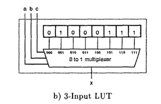
Logic blocks fundamentally are implemented as a series of look-up tables (LUTs). A two-input LUT (LUT2) can simulate any logic gate, noting that the output gate is also configurable (Xilinx and Altera FPGAs typically have one output gate per LUT). These are implemented using a combination of SRAM bits (holding the LUT-mask in configuration memory, CRAM) and a multiplexer (MUX) - in the LUT3 below, the $$a$$, $$b$$, and $$c$$ specify the input to the LUT, with an LUT-mask of 01000111 specifying the output for each corresponding input to the LUT3:
LUTs can be further composed using smaller LUTs and a MUX - below on the left shows a configuration for either two independent LUT5s, or one LUT6. The diagram on the right combines the two concepts:
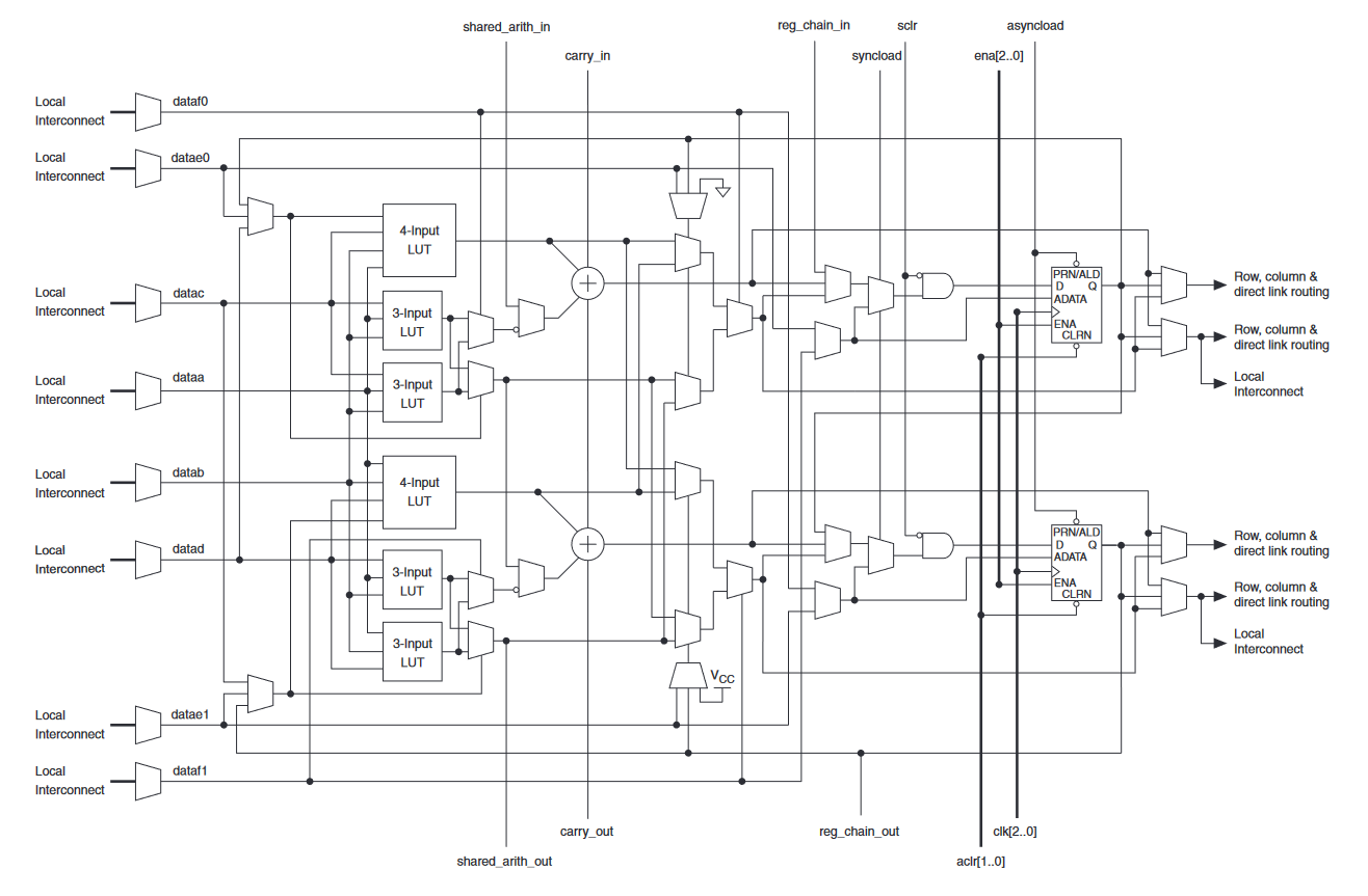
More complex LUTs can be designed to optimize for area/speed, e.g. Altera's Adaptive Logic Module (ALM) that provides an adaptive combinations of LUT3s and LUT4s to share between two LUT5-equivalent logic functions, with additional registers and adders:
LUTs can be connected to flip-flops, together termed as a slice. Flip-flops allow signals to be held for more than a clock-cycle. There are typically different types of slices in an FPGA. Tying them all together is the routing switching matrix to interconnect different Complex Logic Blocks (CLBs) consisting of multiple slices each (for Xilinx FPGAs, SLICEM, SLICEL, and SLICEX that support different functionality for better performance in specialized cases such as arithmetic):
Interconnecting configurable logic blocks
Each CLB contains the LUT, whose output is fanned either directly to the output or into the register, which is selected by the output switch.
Design flow
Typically conducted in a series of steps:
- Design entry: Representing design idea into computerized representation, in the form of Hardware Descriptor Languages (HDLs) which are commonly either Verilog or VHDL (Very High Speed Integrated Circuit HDL).
- Synthesis: Generates a netlist from the HDL using primitives supplied by the FPGA. Usually additionally performs logic optimization, register load balancing (retiming) and other timing performance optimizations (buffering / replication / pipelining / multiplexing).
- Map, Translate, Place and route: Placer determines a place in the chip for each primitive, while router interconnects primitives in order to satisfy timing constraints. Static Timing Analysis (STA) is the most important part, where timing performance is quantified.
- Bitstream generation: Storage of FPGA program in non-volatile flash memory, to be programmed onto the FPGA's SRAM.
Synthesis and place and route tools are typically vendor-specific, though there are also open-source varieties for Lattice (yosys nextpnr) and Xilinx (Project X-Ray), as well as officially-endorsed netlist generation tools (e.g. RapidWright for Xilinx).
This article goes into much further detail on the testing and simulation stages.
High-level design
Two strategies: Register Transfer Level (RTL) or Gate Level modelling. In RTL, behaviours of components are modeled, e.g. what to do when a rising clock edge is detected. In GL, specific components (e.g. NOT or D flip-flops) are specified and directly connected.


