Table of Contents
Serial communication
Consolidated from tidbits in the main log. Description below is specific for ATmega16. Written on 2022-11-05.
Introduction
Serial communication is sending data one bit at a time sequentially over a communication channel. This channel is typically directly a physical layer, where digital values of HIGH/1 and LOW/0 are encoded as voltages.
Serial communication can be performed synchronously, i.e. either a separate clock channel to synchronize sampling times on the receiver or transmission of clock signals during idle time, or asynchronously where the packets are synchronized by start and stop bits in each data frame (packet).
The transmission rate needs to be precoordinated to agree on the frame parameters (e.g. size of data bits, baud rates) before communication can begin - notably there exist schemes where auto-detection of baudrate on the receiver end is implemented to align with that of the transmitter.
Disambiguation
- RS-232 is a physical + link layer protocol, that provides an implementation of serial communication (e.g. the voltage signal levels).
- Symbols / baudrate.
ATmega16 Implementation
The ATmega16 AVR chip provides a USART (Universal Synchronous and Asynchronous serial Receiver and Transmitter) that provides customizability when performing serial communication. It implements both synchronous and asynchronous serial communication.
Physical pins
There are three relevant physical pins for USART:
- TXD pin (Transmit Data, corresponding to Port D pin 1) for transmitter
- RXD pin (Receive Data, corresponding to Port D pin 0) for receiver
- XCK pin (Transfer Clock, corresponding to Port B pin 0) for external clocking
The TXD pin functions as an output pin, while the RXD pin functions as an input pin, switching between HIGH and LOW states. From the electrical characteristics section of the datasheet, for Vcc = 5V,
- HIGH state for voltage input $$V_{IH}$$ > 3V and output $$V_{OH}$$ > 4.2V
- LOW state for voltage input $$V_{IL}$$ < 1V and output $$V_{OL}$$ < 0.7V
Protocol definition
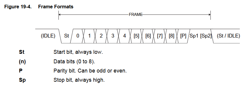
Data is transmitted in serial frames (packets) with the following format, with the definitions encoded in the following register bits:
UCSZ2:0: One character of data bits $$ (n)$$ (ranging from 5 to 9 bits),USBS: Synchronization bits (1 start $$ St$$, and 1 or 2 stop $$Sp$$ bits),UPM1:0: An optional parity bit $$P$$ (even or odd) for error checking
Character bits have little bit-endianness (least-significant bit first). The diagram from the datasheet helps - a frame error (FE) can occur and is detectable only with first stop bit being LOW.
Transmission
In the case of 5 to 8 data bits, transmission is performed by loading the transmit buffer when the data register (transmit buffer) is empty:
USART_TRANSMIT:
	sbis	UCSRA,UDRE	; wait till UDR empty bit set
	rjmp	USART_TRANSMIT
	out	UDR,r16		; load data (e.g. r16) into buffer
	ret
For the special case of 9-bit data, the ninth bit must be written to the TXB8 bit in UCSRB register first, before writing the rest into the UDR. Here we assume data is in r17:r16,
USART_TRANSMIT:
	sbis	UCSRA,UDRE	; wait till UDR empty bit set
	rjmp	USART_TRANSMIT
	cbi	UCSRB,TXB8	; clear 9th bit
	sbrc	r17,0		; skip if bit 0 in r17 is cleared...
	sbi	UCSRB,TXB8	; ... set 9th bit otherwise
	out	UDR,r16		; load data (e.g. r16) into buffer
	ret
Under the hood, the buffered data in the UDR is loaded into the Shift Register for transmission, when there is no ongoing transmission or when the last stop bit of previous frame is transmitted. This Shift Register is needed since the transmission rate (set by baudrate) can vary from the internal clock.
Interrupts can also be used for transmission:
- UDRE Interrupt
- Triggers when UDR is loaded and has not offloaded to Shift Register
- Not automatically cleared when entering interrupt routine
- Enabled by setting UDRIE bit in UCSRB
- Transmit Complete (TXC) Interrupt
- Triggers when entire frame in Shift Register has been shifted out and there is no more data in UDR
- Automatically cleared when entering interrupt routine
- Enabled by setting TXCIE bit in UCSRB
- Useful for half-duplex communication where transmitting application needs to immediately enter receiving mode once transmission complete
Reception
Receiver starts data reception when a valid start bit (LOW) is detected, and starts shifting data into the receive Shift Register. The full frame is then moved into the receive UDR buffer. For 5 to 8 data bits, the following works:
USART_RECEIVE:
	sbis	UCSRA,RXC	; wait until receive complete bit set
	rjmp	USART_RECEIVE
	in	r16,UDR		; store UDR data (e.g. into r16)
For 9 bits, the RXB8 bit needs to be read first before the UDR (which changes the state of the other flags):
USART_RECEIVE:
	sbis	UCSRA,RXC	; wait till receive complete bit set
	rjmp	USART_RECEIVE
	in	r18,UCSRA	; store status (to check for errors)
	in	r17,UCSRB	; store register containing 9th bit
	in	r16,UDR		; store rest of data

	andi	r18,(1<<FE)|(1<<DOR)|(1<<PE)	; check if errors (Z=0)
	breq	USART_RECEIVENOERROR		; no error (Z=1)
	ldi	r17,HIGH(-1)	; error => store -1
	ldi	r16,LOW(-1)
	ret

USART_RECEIVENOERROR:
	lsr	r17		; retrieve RXB8 (UCSRB1) by right-shift...
	andi	r17,0x01	; ...then mask out bit 0
	ret
Similar interrupt available:
- Receive Complete (RXC) Interrupt
- Triggers when UDR buffer contains unread data
- Not automatically cleared when entering interrupt routine
- Enabled by setting RXCIE bit in UCSRB
The three error codes in particular signal errors in receipt:
- Frame Error (FE) bit set when stop bit is not HIGH, e.g. out-of-sync / protocol mishandling
- Data OverRun (DOR) bit set when receive buffer is full (2 characters), receive Shift Register is full (1 character), and a start bit was detected, e.g. serial frames lost
- Parity Error (PE) bit set when next frame in receive buffer has a parity error
If the receive buffer needs to be flushed, read UDR until the RXC flag is cleared:
USART_FLUSH:
	sbis	UCSRA,RXC
	ret
	in	r16,UDR
	rjmp USART_FLUSH
Clock recovery
During asynchronous serial communication, receipt of the start bit in an incoming triggers the receiver clock to align with the frame. The rate at which bits arrive are determined by the user-defined baudrate.
This synchronization process is implemented by a clock recovery logic that oversamples each serial bit and applies a majority vote to the three samples closest to the center of the bit. There are two oversampling configurations available:
- Normal Mode uses 16 samples per serial bit
- Double Speed Mode uses 8 samples per serial bit
Use of three bits to perform majority vote essentially functions like a low pass filter. The central bits are used to avoid sampling near data stream transitions. A graphical representation explains this best:
Note that in double speed mode, there is a larger timing uncertainty to the first zero-sample, which affects the relative phase of the receiver clock to the incoming baudrate, i.e. larger chance of errors.
The same sampling process is applied to the data bits to recover HIGH and LOW states of the data. The stop bit is a little special: the next frame can come immediately after the required central three samples for the first stop bit is performed, so the oversampling rate dictates when the next start bit transition can occur:
The possible early start bit detection positions are marked (A) for Normal Mode, (B) for Double Speed Mode, and (C) for the full stop bit length. Isn't it strange then that there is an option to set 2 stop bits when the second stop bit can be ignored anyway? This is really a workaround to interface with devices that use 1.5 stop bits:
- Transmission will transmit the full 2 stop bits to adhere to the minimally 1.5 stop bit requirement on the receiver
- Receiver can immediately start reading incoming frames arriving after 1.5 stop bits
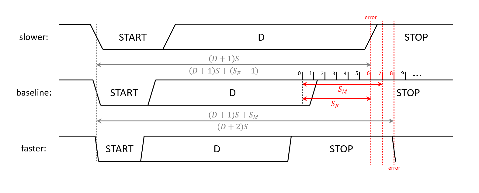
Frequency deviations between the transmitter and receiver can cause problems, with the maximum tolerated errors given by the following table:
To understand the formula, refer to the following diagram I made (central bit positions used below are arbitrary), source:
Receiver clock generation
The last part is devoted to talking about how the clock is generated in the first place. Serial communication can either be synchronized in a master-slave configuration, or asynchronous - set by the UCSRC_UMSEL bit. This determines how the clock is generated for the communication.
- In async mode, can be in normal mode or double speed mode (set by
UCSRA_U2Xbit). - In sync mode, can either be master (with internal clock source), or slave (with external clock source), set by
DDR_XCKregister.
Serial clock calculation
- Clocking to USART achieved using a down-counter, which also loads with the USART Baud Rate Register (UBRR) value when the counter reaches zero, i.e. the number of cycles is UBRR + 1.
- Clock generated whenever counter reaches zero, so the base clock output is (f_osc/(UBRR+1)).
- Transmitter then further divides by 16 in asynchronous normal mode, for data sampling purposes as mentioned above.
$$$$ \text{baud} = \frac{f_{osc}}{16(\text{UBRR}+1)} \quad\Rightarrow\quad{} \text{UBRR} = \frac{f_{osc}}{16\text{baud}} - 1 $$$$
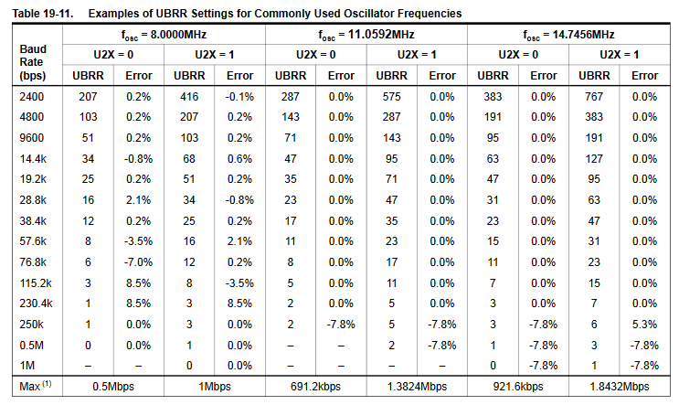
This in the end gives the following error rates, when attempting to communicate with a transmitter at the listed common baudrates. This gives a measure of how much error is being induced, and thus what frame size should be used.


