


projects:electronics:fpga:log
Log
2023-08-23 Wednesday
Some coding tips from CG3207:

2023-01-24 Tuesday
Taking cues from the LCMXO2-7000HE-B-EVN board (TQFP-144 form factor), the design included an FTDI FT2232HL USB to JTAG/RS232 chip for programming/interfacing over USB.
LCMXO2-7000HE-B-EVN schematics
A rough guide to what the MachXO2 chip can support:
- SRAM-based Programmable Logic Device (PLD)
- i.e. active configuration which defines the behaviour of the FPGA
- Includes an internal Flash memory to make device appear non-volatile
- Configuration from internal Flash PROM
- User Flash Memory (UFM)
The configuration flow1)
in particular is illuminating with respect to the use of PROGRAMN, INITN and DONE lines. Note that INITN and DONE are bidirectional, open-drain2) I/O only when enabled. A summary of the flow:
- During power ramp, a Power On Reset (POR) circuit monitors state until VCC > 2.1V before releasing an internal reset strobe to trigger initialization.
INITNis asserted active-low (i.e. open-drain pulled high when inactive) andDONEis driven low.
- Up until (1)
tINITLtime period has elapsed, (2)PROGRAMNpin is deasserted, (3)INITNis not asserted low by an external master, FPGA remains in an initialization state which clears SRAM - After which follows the configuration state, where the MachXO2 fetches configuration data from non-volatile memory, usually the internal Flash. An asserted low
INITNsignals an error in configuration - During wake-up state, (1) output pins are permitted to be released from initial high-Z state, (2) internal Global Set/Reset (GSR) enabled, (3) disables write to RAM with another internal strobe, (4) assert the DONE pin
- Finally, user mode is reached, which runs the programmed logic. Reinitialization occurs when: (1)
PROGRAMNinput pin is asserted, (2)REFRESHcommand received through one of FPGA's configuration ports, (3) power cycling.REFRESHin particular is useful for hot-reloading of Flash memory.
The Feature Row exists, which seem to behave similar to the functionality of MCU FUSES. The MachXO2 Programming and Configuration guide also specifies the following options for programming:
- 1149.1 JTAG
- Self-download
- Slave SPI
- Master SPI
- Dual Boot
- Inter-Integrated Circuit (I2C)
- WISHBONE bus
Description follows:


JTAG port is enabled by default, with the following configuration:


and finally, the benefits of using JTAG interface:

This article talks about using the JTAG interface for its original purpose, for boundary-scan during testing:


Question now is, how does one program over the JTAG interface? Seems like there is no well-defined protocol to achieve this, see Electronics SO. And this is indeed the case: the flash programming steps are defined in section 10 of the configuration datasheet, under "10.1 Flash Programming". File formats supported seem to be MachXO2-defined JEDEC file format, STAPL, SVF or a hex/binary bitstream.
This looks like it might be super useful for understanding how JTAG works.
2023-01-22 Sunday
Some miscellaneous software to install: fxload
Getting myself a head-start using existing FPGA repositories, by listing the process used there. Infrastructure entails the following connections for writing firmware to the FPGA via the microcontroller (MCU):
| 7C68013A | 1200HC |
|---|---|
| PA5/FIFOADR1 | PT10C/TDO |
| PA4/FIFOADR0 | PT10D/TDI |
| PA0/INT0 | PT11C/TCK |
| PA1/INT1 | PT11D/TMS |
| +3.3V | PT15C/JTAGENB |
For Atmel MCUs:
avr-gcc: cross compiler to compile MCU firmwaredfu-programmer: interface with MCU in DFU mode (available with in-built Atmel bootloader)jtagprog: internal, firmware for MCU to act as FPGA programmer for FPGA (JTAGMODE to exit the initial boot CDC interface)usbprog: internal, driver to recognize JTAG programmer interface of MCU- Might need
dkmsto install driver, see SO
jtagprg: internal, interface with JTAG programmer to upload firmware to FPGA, parser for SVF
Additionally, for Cypress MCUs:
sdcc: compiling firmware into Intel hex formatfxload: loading firmware onto chipusbjtag: internal, firmware for MCU to act as FPGA programmer
So far doesn't seem to be working:
Plain MCU does not respond, but eventually does after disconnecting other devices from hub
2023-01-19 Thursday
The assign statement essentially drives a wire (which is initially unconnected) at the driven logical level. In a module, the input wires are assumed to be externally driven, which we then rely on to drive the output. Note that inputs to modules must be wires, and if input/output datatype is not specified they are assumed to be wires as well of one-bit width (if the wire is not declared at all, it is also assumed to be a 1-bit width wire - disable this behaviour with the directive `default_nettype none):
module andGate(
    input a,   // wire
    input b,   // wire
    output c,  // wire
)
assign c = a & b;
endmodule

// or equivalently, in Verilog-1995
module andGate(a, b, c);
input a, b;
output c;
assign c = a & b;
endmodule
There is the concept of blocking = and non-blocking <= assignments in an always block. This article explains non-blocking assignment nicely, using a twisted ring counter3), reproduced here. The intended behaviour of a twisted ring counter is achieved by using non-blocking assignment, which performs "assignment scheduling" - in other words the new value is not updated until the end of the cycle, and takes on the last assigned value:
// 2-bit twisted ring counter
// { q_dff1, q_dff2 }: 10 -> 11 -> 01 -> 00 -> ...
always @(posedge clock) begin  // run on every positive clock edge
  q_dff1 <= ~q_dff2;  // inversion assigned after cycle finishes
  q_dff2 <= q_dff1;
end
When using blocking assignment, values are immediately assigned as the statements are reached (i.e. continuous assignment). This means the following two always blocks are equivalent:
always @(posedge clock) begin
  q_dff1 = ~q_dff2;  // q_dff1 is immediately assigned the inverse of q_dff2...
  q_dff2 = q_dff1;   // ...so q_dff2 is assigned ~q_dff2
end

// equivalent circuit, which corresponds to a 1-bit twisted ring counter
// { q_dff2 }: 1 -> 0 -> ...
// q_dff1 is equivalent to q_dff2, so there is no need for a flip-flop
always @(posedge clock) begin
  q_dff2 <= ~q_dff2;
end
assign q_dff1 = q_dff2;
Small caveat: blocking and non-blocking statements cannot be used for the same signal. Note also that with blocking assignments, one can have combinational design inside an always block as well. As to why it's called blocking and non-blocking, see this SO answer for the most illuminating explanation I've ever seen4).
There are also if - else if - else constructs and case constructs that are similar to that of C:
// 2-bit multiplexer with if-else
always @(s) begin
  if (s == 2'b00)
    begin
      y = i0;
      z = ~z;
    end
  else if (s == 2'b01)
    y = i1;
  else if (s == 2'b10)
    y = i2;
  else
    y = i3;
end

// 2-bit multiplexer with case (and more efficient to boot, using a single LUT)
always @(s) begin
  case (s)
    2'b00   :
      begin
        y = i0;
        z = ~z;
      end
    2'b01   : y = i1;  // using binary
    2       : y = i2;  // using integer
    default : y = i3;  // using default case
  endcase
end
Loops are available as well, though mainly for use in testbenches (recall that the whole always block fully executes before values are updated, this means the synthesized loops will simply reflect the last assigned value after a single cycle). Use cases of for loops is typically to group different assignments on different outputs, see below:
// forever loop
forever begin
   ...
end

// repeat loop (fixed number of times)
repeat (5) begin
   ...
end

// for loop
for (i = 1; i < 4; i = i + 1) begin
    shift[i] <= shift[i-1];
end

// while loop
i = 1;
while (i < 4) begin
    shift[i] <= shift[i-1];
    i = i + 1;
end
A quick note that VHDL and Verilog can be interchanged, following the usual rules of port mapping when using VHDL modules in Verilog.
2023-01-18 Wednesday
This two resources are pretty good at giving further insights on the design flow and abstraction layers.
A quick syntax overview of Verilog: there is the 1995 standard, and the 2001 standard. Described here will be the 2001-standard to fully capture most features (what is backward compatibility when the specification is >20 years old?). Here's a nice reference guide for Verilog-2001 by Sutherland HDL. In the style of LearnXinYminutes, assuming knowledge of C, and content adapted from ChipVerify:
// Single line comment
/* Multi-line comment
 */

// Verilog is similar to C syntax: (1) case-sensitive, (2) ;-terminated.
// Numbers denoted [size]'[format][number], where size is number of bits
// The following are all the number decimal 10, underscores legal:
4'b1010 = 4'd10 = 4'10 = 4'o12 = 4'hA = 4'b1_010;

// Default format is decimal, default size is datatype size, negation in front
integer a = -10;   // decimal 10
integer a = -'hA;  // 32-bit integer by default

// Values are 4-state, whose actual voltages model that of the hardware:
//   0 represents logical zero / false
//   1 represents logical one / true
//   X represents unknown logical value (not "don't care")
//   Z represents high impedance state, default if unconnected

// Strings as per C-style
// Identifiers must follow regex ^[A-Za-z_][A-Za-z0-9_$]*$ and not collide with keywords
Conventions for datatypes in timing diagrams and simulator waveforms are as follows:

Nets simply connect between hardware entities, and do not store values. Used to convey signal strength from connected components. A wire is the most commonly used type of net, representing an electrical wire:

wire my_wire1;
wire [3:0] my_wire2;  // 4-bits wide (4 wires), from bit 3 to bit 0

// Other net datatypes include: tri, wand, supply0, ...
Variables represent an abstraction of data storage element. Several options available:
reg [3:0] z = 3'b010;  // general register, can be any size (default size 1)
integer   a = 109;     // signed 32-bit number
time      b = 50ns;    // unsigned 64-bit number (to represent time)
real      c = 40.25ps; // 64-bit float
realtime  d = 4.32;    // 64-bit float (to represent time)

// Strings can be stored, truncating or padding (with spaces) from the left:
reg [8*11:0] str = "Hello world";
Multi-bit nets and variables are known as vectors (as opposed to single bit scalars). Reads/Writes similar to C-style arrays (and Python numpy array writes), with the notable difference from out-of-bounds vector accesses returning X.
reg [3:0] addr = 4'b0Z00;
addr [2:1] = 2'b1X;  // addr is now 4'b01X0
addr [2];  // returns 1
Arrays can be declared for reg, wire, integer and real types. Array access is similar to C-style arrays. A 1D array of reg variables is referred to as memory:
reg       y1 [3:0];       // scalar reg 1D array of depth 4, aka memory
reg [7:0] y2 [3:0][1:0];  // 8-bit reg 2D array of rows 4 and columns 2
Operators follow a mix of C and Python styles:
Arithmetic:  +, -, *
             /, %, **  (may not synthesize)
Bitwise:     ~, |, &, ^, ~&
Relational:  >, <, >=, <=, ==, !=
Logical:     !, ||, &&
Conditional: ? :
Shift:       >>, << (logical shift)
             >>>, <<< (arithmetic shift, MSB filled)
Sign-change: $unsigned(), $signed()
Concatenation: {}, {{}}
The concatenation and replication operators combine smaller vectors into larger vectors:
wire [1:0] a = 2'b01;
wire [2:0] b = 3'b0X1;
wire [7:0] c;

assign c = { 1'bZ, {2{a}}, b };  // c = 8'bZ01010X1
assign { c[7:6], c[5:0] } = { 1'bZ, {2{a}}, b };  // also valid


// convention is little-endian, cannot swap endianness once declared
wire [3:0] w = 4'b01XZ;
// invalid: assign w = w[0:3];

// for vector reversal, use the concatenation instead
assign w = { w[0], w[1], w[2], w[3] };

// alternatively with for loops,
always @(*) begin
    for (integer i = 0; i < 4; i++)
        w[i] = w[3-i];
end

// or using a generate-for loop,
generate
    genvar i;
    for (i = 0; i < 4; i++) begin: block_name
        assign w[i] = w[3-i];
    end
endgenerate
localparam, parameter and defparam are used to set constants (latter two for structural modeled code). Syntax for localparam is localparam N = 2, P = 3;.
Modeling styles
There are four modeling styles when writing Verilog code:
- Design with continuous assignment statements
- Structural design
- Design with procedural assignment statements
- Mixed design
When using continuous assignment statements, instead of explicitly specifying the structure of the design, the relationship between signals are defined instead.
- comparator2Bit.v
module comparator2Bit(
    input wire[1:0] a, b,
    output wire eq
);
wire[3:0] s;
assign s[0] = ~a[1] & ~a[0] & ~b[1] & ~b[0];
assign s[1] = ~a[1] &  a[0] & ~b[1] &  b[0];
assign s[2] =  a[1] & ~a[0] &  b[1] & ~b[0];
assign s[3] =  a[1] &  a[0] &  b[1] &  b[0];
assign eq = s[0] | s[1] | s[2] | s[3];
endmodule

Structural modeling uses composition to assemble larger designs.
- comparator1Bit.v
module comparator1Bit(
    input wire x, y,
    output wire eq
);
wire s0, s1;
assign s0 = ~x & ~y;
assign s1 = x & y;
assign eq = s0 | s1;
endmodule
- comparator2BitStruct.v
module comparator2BitStruct(
    input wire[1:0] a, b,
    output wire eq
);
wire s0, s1;
comparator1Bit eq_bit0 (.x(a[0]), .y(b[0]), .eq(s0));
comparator1Bit eq_bit1 (.x(a[1]), .y(b[1]), .eq(s1));
assign eq = s0 & s1;
endmodule


Using procedural statements involve nesting them within an 'always' block. These statements are run sequentially, so the order of the statements matter. This contrasts with the 'always connected' wires in the continuous assignment strategy where statements are executed in parallel.
- comparator2BitProcedure.v
module comparator2BitProcedure(
    input wire[1:0] a, b,
    output reg eq
);
always @(a,b)    // sensitivity list
                 // block executes iff there are changes in 'a' and/or 'b'
begin
    if (a[0]==b[0] && a[1]==b[1])
        eq = 1;
    else
        eq = 0;
end
endmodule

Finally, a mixed design philosophy is also supported:
- comparator2BitMixed.v
module comparator2BitMixed(
    input wire[1:0] a, b,
    output wire eq
);
reg[1:0] s0, s1;

always @(a,b)
begin
    if (a[0]==b[0])
        s0 = 1;
    else
        s0 = 0;
end

always @(a,b)
begin
    if (a[1]==b[1])
        s1 = 1;
    else
        s1 = 0;
end
assign eq = s0 & s1;
endmodule
Design philosophy
Digital design mainly one of two methods:
- 'Combinational design' where the output only depends on the present value of the inputs, and does not require memory. This can be implemented purely with logic gates. This is analogous to a stateless "pure" function.
- 'Sequential design' where the system is stateful, i.e. depends on both the current inputs and the previous state of the system. Memories are needed, which are implemented with flip-flops.
The following diagram summarizes pretty much everything:

While the complete design can be written using purely sequential statements, the resulting hardware may be too complex or may not even synthesize. Best is to construct small units then piece them together with structural modeling.
This looks like a good guide: VerilogGuide.
2023-01-17 Tuesday
The vendor synthesis tool actually serves as a pretty useful tool for looking up different chip specification (and what they mean) too. See for example the MachXO2 chip we use, with part number LCMXO2-2000HC-6TG100I:

2023-01-10 Tuesday
Still trying to identify how to even take the first step towards programming on an FPGA. How is Verilog related to FPGA, other than it just being the language for describing circuits?
Some things I can consider doing:
- Try out the 182 guided problem sets on Verilog, which uses Icarus as the backend: HDLbits. Username is currently "pyuxiang".
Some things I think I learnt:
- Lattice Diamond and Xilinx Vivado are synthesis tools as well as place-and-route tools. This tool is required to actually deploy circuits onto the chip itself (probably by generating and uploading of the bitstream), as well as the synthesis itself.
- Simulator tools on the other hand can be used to simulate the behaviour of a particular piece of code. There are many options for this.
- Designing of a testbench to test a design is almost as hard as designing the circuit under test.
The workflow for designing FPGAs is aptly described in asic-world tool page, and adapted here (highly recommend to give the page a read though - it has illustrative diagrams):
| Stage | Description | Format | Tool |
|---|---|---|---|
| Specification | Specification of important parameters in system, e.g. a counter with 4-bit wide bus, have synchronous reset, etc. | Text | - |
| High-level design | Splitting of design into blocks based on function, e.g. registers, ALU, instruction decode, etc. | Text + Waveform drawings | GTKWave (free) |
| Low-level design | Description of how each block is implemented, e.g. state machines, counters, mux, decoders, internal registers. | ||
| RTL coding | Writing code itself | HDL code | Covered (code coverage, free) |
| Simulation | Verifying functional characteristics by writing a testbench which generates clk, reset and other required test vectors. Waveform output is validated. Timing simulation performed after synthesis and P&R for timing validation | Simulators | ModelSim (popular, commercial) VCS (fastest, commercial), Verilog-XL (the standard sign-off, commercial), Icarus (open-source) |
| Synthesis | Conversion of RTL and constraints into target technology primitives, with formal verification to check if RTL to gate mapping is correct | Synthesizers | Xilinx Vivado (for Xilinx) Lattice Diamond (for Lattice) Synopsys Design Compiler (commercial) |
| Place & Route | Netlist generated from synthesis is used to place gates and route the clock tree/reset (GDS output in the case of ASICs) | P&R tools | Typically use FPGA vendors' P&R tools. |
| Post-Si validation | - | Chip | Testing with actual board and chip, require device drivers |
Side-note: Schematic generation is usually not a common thing to do in FPGA design, since it's more behavioural. For schematic generation, can either perform using Xilinx Vivado or yosys - these are synthesis tools since the HDL needs to be converted into gates, etc. See the following tutorial using yosys.
Consider reading EDA Playground's settings to see what options are available.
2)
A reminder of open-drain configuration that uses an n-type MOSFET as a switch by connecting the drain to an external pullup to a high voltage source (when MOSFET low, external circuit is driven HIGH; MOSFET high acts like a short which pulls the external circuit LOW). This allows the FPGA to only assert LOW, but not actively drive the pin HIGH/LOW.
3)
Recall that a ring counter cycles the sequence using a series of chained flip-flops, i.e. given an initial state of
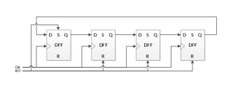
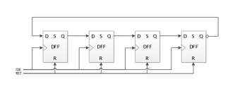
4'b1000 in a 4-bit ring counter, the sequence follows the cycle: 
1000 -> 0100 -> 0010 -> 0001 -> ...In a twisted ring counter, a NOT gate is present at the output of the last flip-flop, i.e. given the same initial state of
4'b1000 in a 4-bit twisted ring counter, the sequence instead follows: 
1000 -> 1100 -> 1110 -> 1111 -> 0111 -> 0011 -> 0001 -> 0000 -> ...


projects/electronics/fpga/log.txt · Last modified: 3 years ago (30 August 2023) by justin