Xilinx Vivado
No other way but to play around with toy examples to have a better sense of what is going on...
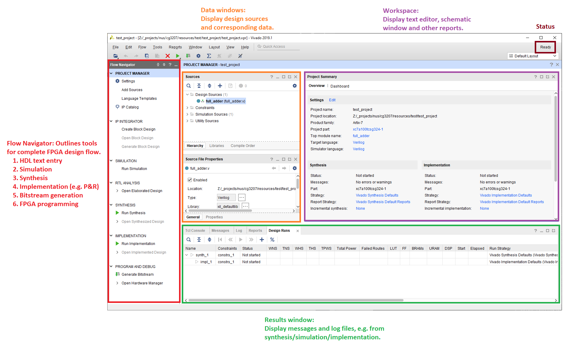
Installed Vivado 2019.1 (found under the Vivado Archives in their Downloads webpage), more specifically "Vivado Design Suite - HLx Editions - 2019.1". The version chosen is to align with existing projects I'm working with, i.e. CG3207 course. This installers works for both Windows and Ubuntu.
We can create a new project under Vivado with the following selections in their Wizard:
- Project type: RTL Project (i.e. the whole source + synthesis setup)
- Target and simulator language: Verilog
- Add sources: Create new file and specify top level, e.g.
full_adder- This creates the Verilog source file found under
{{ROOT}}/{{PROJECT}}.srcs/sources_1/new/full_adder.v
- Add constraints: Ignore this for now
- Default part: Select the FPGA chip you have for the project, e.g.
xc7a12t-ics325-1L
Once we click on Finish, the project will open up and a prompt will appear to request specification of module name (i.e. same as the source file, full_adder) and the input and output ports. Went for:
| Port name | Direction |
|---|---|
| A | input |
| B | input |
| CIN | input |
| SUM | output |
| COUT | output |
- full_adder.v
module full_adder(
    input A,
    input B,
    input CIN,
    output reg SUM,
    output reg COUT
    );

    reg p, g;  // internal signals

    // LHS assignments in always blocks must be declared registers,
    // but that does not mean it always synthesizes to a register in hardware
    always @(A, B, CIN)
        begin
            p = A ^ B;
            g = A & B;
            SUM <= p ^ CIN;
            COUT <= g | (p & CIN);
        end

endmodule
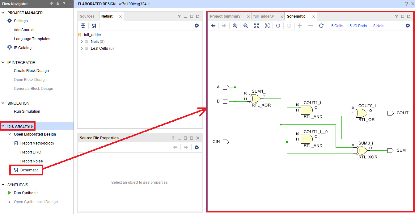
Under RTL analysis, the schematic representation (independent of the technology library / target device) is calculated and displayed. One can right-click on individual components and select "Go to Source" to see why it was elaborated as such.
Under Sources tab in the Project Manager, click the plus sign to create a simulation source, and name it test_full_adder. Note that no I/O ports need to be defined since the testbench is not meant to be synthesized for physical hardware. This file test_full_adder.v is the testbench.
- test_full_adder.v
// time unit of 1ns with precision of 1ps
`timescale 1ns / 1ps

module test_full_adder(

    );

    // declare inputs
    reg A;
    reg B;
    reg CIN;

    // declare outputs
    wire SUM;
    wire COUT;

    // instantiate device-under-test
    // i.e. object 'dut' of type 'full_adder' with following parameters created.
    full_adder dut(A, B, CIN, SUM, COUT);

    // stimuli as part of test
    // initial is only used for testbenches
    initial
        begin
            A = 0; B = 0; CIN = 0; #10;  // # is the delay statement
            A = 0; B = 0; CIN = 1; #10;  // which delays for 10 time units
            A = 0; B = 1; CIN = 0; #10;
            A = 0; B = 1; CIN = 1; #10;
            A = 1; B = 0; CIN = 0; #10;
            A = 1; B = 0; CIN = 1; #10;
            A = 1; B = 1; CIN = 0; #10;
            A = 1; B = 1; CIN = 1; #10;
        end

endmodule
Under Simulation, click on "Run Behavioural Simulation". The simulation window will pop out, which you can zoom in and out using Ctrl-Scroll.


